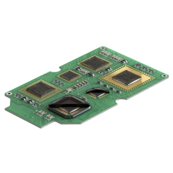
Semiconductor Packaging
Innovative Materials for Evolutionary Electronics Capability

Semiconductor technology and, specifically, the packaging of semiconductor devices has never touched more applications than it does today. As all parts of everyday life become increasingly digitalized – from automobiles to home security to smartphones and 5G infrastructure – semiconductor packaging innovation is at the core of responsive, reliable, robust electronic functionality.
Thinner wafers, decreasing footprints, finer pitches, package integration, 3D designs, wafer-level technology and high-volume production economies of scale demand enabling materials that can support innovation ambitions. Henkel’s total solutions approach leverages extensive global resources to deliver superior semiconductor packaging material technologies and cost-competitive performance. From die attach adhesives used in traditional wirebond packaging to advanced underfills and encapsulants for advanced packaging applications, Henkel provides the cutting-edge materials technology and global support top microelectronics companies require.